
 EN
EN ES
ES ITA
ITA DE
DE FR
FRLock-in Amplifier Sensitivity: Why a 1 nV Specification Doesn't Guarantee 1 μV Detection

Why Can't You Measure a 1 μV Signal with a Lock-in Amplifier Rated at 1 nV Sensitivity?
The Hidden Conditions Behind a 1 nV Noise Floor
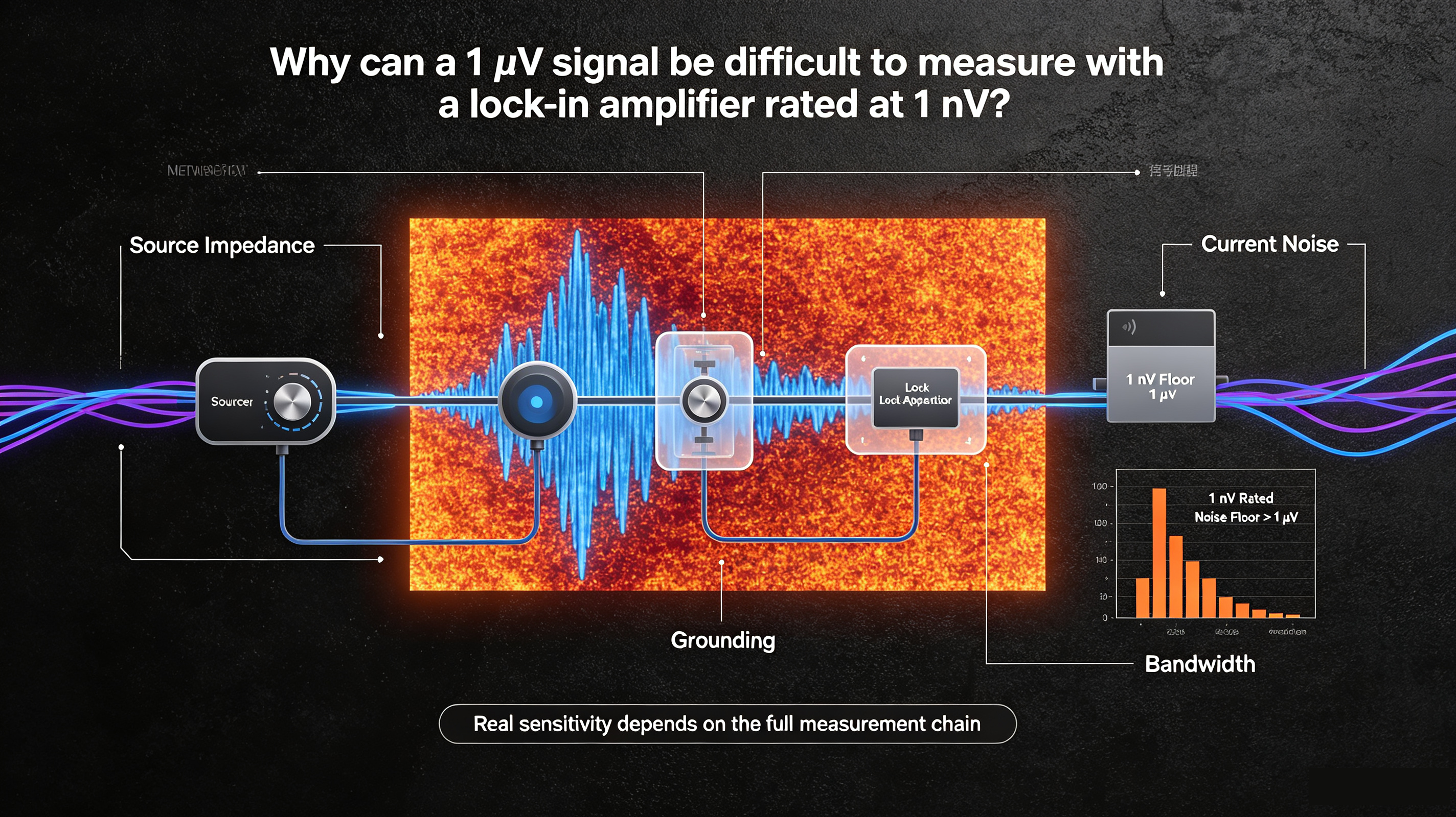
Your lock-in amplifier datasheet says it has a 1 nV detection limit.
You connect a 1 μV signal to the input, expecting an easy measurement.
After all, 1 μV is 1,000 times larger than 1 nV.
But the signal-to-noise ratio is still less than 3—or the signal cannot be reliably distinguished from the noise at all.
Is the instrument defective?
Usually, no.
The problem is that the 1 nV specification is measured under highly optimized conditions, and your actual experiment may satisfy very few of them.
In real-world measurements, source impedance, input current noise, electromagnetic interference, and measurement bandwidth can all increase the effective noise floor.
The result is a fundamental but often overlooked principle:
The sensitivity specified on a lock-in amplifier datasheet is not necessarily the minimum signal you can measure in a real experimental setup.
1. What Does the "1 nV" Specification Actually Mean?
A lock-in amplifier's sensitivity or minimum detectable signal is normally characterized under carefully controlled conditions.
The source material identifies four important conditions behind the 1 nV-level specification:
Source impedance below 1 kΩ, approaching a short-circuit input
Differential input configuration with good shielding
Long time constant, typically on the order of seconds
Very low external electromagnetic interference, such as inside a shielded enclosure
These conditions are very different from many practical optical or photodetection experiments.
For example, a real photodetector may have a source impedance ranging from kΩ to MΩ, while the measurement may need a short time constant for real-time scanning.
At the same time, the experiment may be exposed to:
50 Hz mains interference
Harmonics
Ground loops
Cable pickup
Electromagnetic coupling
Each of these effects adds to the noise budget.
The result is that a nominal 1 nV instrument noise floor can become a much higher system-level detection limit.
2. First Layer: Source Impedance and Johnson Noise
One of the most important factors is the impedance of the signal source.
Real optical detectors—including:
Photodiodes
Photovoltaic cells
Thermopiles
can have source impedances ranging from relatively low values to several megaohms.
Every resistor generates thermal or Johnson noise.
The RMS voltage noise spectral density can be expressed as:
vn = √(4kTRΔf)
where:
k is Boltzmann's constant
T is absolute temperature
R is source resistance
Δf is measurement bandwidth
For a 1 MΩ source impedance at 300 K, the source material gives approximately:
vn ≈ 128 nV/√Hz
Even with only a 1 Hz bandwidth, the Johnson noise is therefore approximately:
128 nV RMS
This is already 128 times higher than 1 nV.
If the source impedance increases to 10 MΩ, the thermal-noise contribution increases further.
This leads to a simple but critical relationship:
Higher source impedance → higher Johnson noise → higher practical detection limit.
Therefore, comparing a real 1 MΩ detector directly with a datasheet sensitivity measured using a near-zero-impedance source can be misleading.
3. Second Layer: Input Current Noise Becomes Voltage Noise
Source impedance creates another problem.
A lock-in amplifier's input stage has not only voltage noise but also input current noise.
The source material uses approximately:
2.5 fA/√Hz
as a representative input current-noise value for a Zurich Instruments MFLI.
When this current noise flows through a 1 MΩ source impedance, it produces an equivalent voltage-noise component:
2.5 fA/√Hz × 1 MΩ = 2.5 nV/√Hz
This contribution becomes increasingly important as source impedance increases.
In simplified form:
vn,current = in × Rsource
Therefore:
Higher source impedance → larger current-noise-induced voltage noise
This is why selecting a lock-in amplifier based only on its input voltage-noise specification can lead to disappointing real-world performance.
For high-impedance sources, the input current-noise specification can be just as important—or even more important—than the voltage-noise specification.
4. Third Layer: Grounding and Common-Mode Interference
Even if the intrinsic electronic noise is extremely low, environmental interference can overwhelm a microvolt-level signal.
A typical laboratory environment contains strong 50 Hz mains interference and harmonics.
The source notes that the amplitude of such interference can reach the mV level.
Now compare:
Interference = 1 mV
Signal = 1 μV
The interference is:
1,000× larger than the signal.
At first glance, a lock-in amplifier with a common-mode rejection ratio (CMRR) of 120 dB appears more than capable of handling the problem.
The idealized residual would be:
1 mV / 10120/20
= 1 mV / 10⁶
= 1 nV
However, this calculation assumes near-perfect differential matching.
Real experimental setups are rarely perfect.
Common-mode rejection can deteriorate because of:
Cable asymmetry
Source-impedance mismatch
Ground loops
Unequal signal paths
Poor shielding
The source also highlights the use of guarding and Kelvin connections as standard techniques for improving low-level measurements.
Therefore, extracting a 1 μV signal from a 1 mV interference environment requires approximately 1,000:1 suppression of the unwanted signal.
Even small imperfections can consume a significant portion of the available noise margin.
5. Fourth Layer: Time Constant and Measurement Bandwidth
This is one of the most important—and most frequently overlooked—factors.
A lock-in amplifier improves signal-to-noise ratio by narrowing its effective measurement bandwidth.
In other words:
A lock-in amplifier trades measurement speed for noise performance.
The source associates a 1 nV-level sensitivity specification with a time constant on the order of 1–3 seconds, corresponding to a very narrow equivalent noise bandwidth (ENBW).
For a first-order low-pass filter, a commonly used approximation is:
ENBW ≈ 1/(4τ)
For example, with:
τ = 1 s
the ENBW is approximately:
0.25 Hz
For:
τ = 10 ms
the bandwidth increases to approximately:
25 Hz
The ratio is:
25 / 0.25 = 100
Therefore, the white-noise RMS level increases by approximately:
√100 = 10×
This illustrates the fundamental trade-off:
Shorter time constant → wider bandwidth → more noise
Longer time constant → narrower bandwidth → less noise
The source emphasizes that when an experiment requires rapid measurement—for example, scanning or imaging—the time constant must often be reduced, causing the effective detection limit to deteriorate rapidly.
6. Putting the Noise Sources Together
Consider a representative photodetection experiment.
The source gives the following approximate noise contributions:
| Noise Source | Representative Contribution |
|---|---|
| 1 MΩ source Johnson noise | 128 nV/√Hz |
| Input current-noise conversion | 2.5 nV/√Hz |
| Residual common-mode interference | ~50 nV/√Hz |
| Instrument voltage noise | 2.5 nV/√Hz |
Assuming these noise sources are statistically independent, the total input-referred noise can be estimated using the root-sum-square method:
vtotal = √(v₁² + v₂² + v₃² + v₄²)
Using the values above:
vtotal ≈ √(128² + 2.5² + 50² + 2.5²)
≈ 138 nV/√Hz
Now assume:
τ = 100 ms
The corresponding ENBW is approximately:
2.5 Hz
The total RMS noise is then approximately:
138 nV/√Hz × √2.5 Hz
≈ 218 nV RMS
For a:
1 μV signal
the approximate signal-to-noise ratio becomes:
1 μV / 218 nV ≈ 4.6
So the signal is measurable—but only marginally.
This is a far cry from the intuitive assumption that:
1 μV / 1 nV = 1,000
therefore the signal should be extremely easy to measure.
The difference comes from the fact that 1 nV is not the noise level of your entire experimental system.
7. Why the Datasheet Number Can Be Misleading
The fundamental mistake is comparing two different things:
Datasheet sensitivity
Measured under:
Low source impedance + narrow bandwidth + excellent shielding + optimized input configuration
versus:
Real experimental detection limit
Determined by:
Source noise + input current noise + environmental interference + measurement bandwidth + instrument noise
The second quantity is what actually determines whether your 1 μV signal can be measured reliably.
This distinction is especially important in:
Optical detector measurements
Photodiode experiments
Fiber optic sensing
Precision spectroscopy
Weak-signal photonics experiments
Low-frequency measurements
High-impedance sensor systems
8. How to Improve the Real-World Detection Limit
8.1 Reduce the Effective Source Impedance
This is often the first parameter to investigate.
Possible approaches include:
Adjusting the photodetector operating point
Adding a low-noise buffer amplifier
Using a JFET-input amplifier with very low bias current
Using transformer coupling where appropriate
The objective is to prevent a high source impedance from converting input current noise into a significant voltage-noise component.
For a high-impedance detector, a suitable buffer stage can therefore make a major difference.
9. Use a Longer Time Constant When Possible
If measurement speed is not critical, increasing the time constant is one of the simplest ways to reduce noise.
The source recommends maintaining a time constant around:
τ ≥ 300 ms
where practical, instead of aggressively reducing it to values such as 10 ms.
The trade-off is straightforward:
Longer τ → narrower ENBW → lower noise → better SNR
but:
Longer τ → slower response
Therefore, the correct time constant should be determined by the dynamics of the measurement rather than by the desire for maximum sensitivity alone.
10. Fix the Grounding Before Blaming the Instrument
For microvolt-level measurements, grounding is part of the measurement system.
Practical measures include:
Use a single-point grounding strategy
Minimize ground-loop area
Use twisted and shielded signal cables
Keep sensitive signal wiring away from mains wiring
Consider galvanic isolation when necessary
The source specifically identifies ground loops and imperfect shielding as major factors that can degrade common-mode rejection.
A sophisticated instrument cannot compensate indefinitely for poor system-level noise control.
11. Do Not Select a Lock-in Amplifier by Voltage Noise Alone
When evaluating a lock-in amplifier for a high-impedance sensor, at least four specifications should be considered together:
1. Input voltage noise
How much intrinsic voltage noise does the input stage generate?
2. Input current noise
How much current noise is injected into the source?
3. Source impedance
How strongly does the detector convert current noise into voltage noise?
4. Effective noise bandwidth
How much bandwidth is actually required by the experiment?
A simplified model is:
Total noise ≈ f(voltage noise, current noise × source impedance, source noise, environmental interference, bandwidth)
This system-level approach is much more meaningful than comparing a single headline sensitivity number.
12. The Practical Measurement Chain Matters More Than the Headline Specification
A lock-in amplifier is an extremely powerful tool for weak-signal detection.
But it does not violate the laws of noise physics.
Its performance depends on the complete measurement chain:
Sensor → Source impedance → Cable → Input stage → Grounding → Filtering → Time constant → Demodulation
If any stage introduces significant noise, the final detection limit can be much worse than the instrument's headline specification.
This is particularly important when working with microvolt- or nanovolt-level signals.
13. Conclusion
If your lock-in amplifier is rated at 1 nV sensitivity, but your 1 μV signal is still difficult to detect, the instrument is not necessarily underperforming.
The key question is:
Under what conditions was the 1 nV specification obtained?
In a real experiment, several factors can increase the effective noise floor:
1. Source impedance
High resistance produces Johnson noise and converts input current noise into voltage noise.
2. Common-mode interference
Mains interference, ground loops, cable asymmetry, and imperfect shielding can overwhelm microvolt-level signals.
3. Measurement bandwidth
A shorter time constant increases ENBW and therefore increases the integrated noise.
4. Instrument noise
The lock-in amplifier's own voltage and current noise still contribute to the overall noise budget.
The most important lesson is:
The datasheet sensitivity is an instrument specification; the practical detection limit is a system specification.
For low-level measurements, the right approach is therefore not simply to buy an instrument with a smaller number on the datasheet.
Instead:
Reduce source impedance → minimize current-noise conversion → control grounding → narrow the measurement bandwidth → optimize the complete signal chain.
A 1 nV lock-in amplifier may be capable of detecting extremely weak signals—but only when the rest of the experiment allows that performance to emerge.