
 EN
EN ES
ES ITA
ITA DE
DE FR
FRWhy Is Spectrometer Resolution Worse Than the Datasheet Specification?

Why Does a 0.05 nm Spectral Peak Measure 0.3 nm on a Spectrometer Rated at 0.1 nm?
The Hidden Resolution Bottleneck: Entrance Slit Width
Many optical engineers assume that spectral resolution is an intrinsic parameter of the diffraction grating.
If a spectrometer is specified with a resolution of 0.1 nm, it seems reasonable to expect it to resolve a 0.1 nm spectral feature.
But in practice, you may encounter a very different result:
A laser spectral line with an actual 0.05 nm FWHM is measured as approximately 0.3 nm, while two peaks separated by 0.15 nm appear as a single broad peak.
Is the diffraction grating inadequate?
Not necessarily.
In many practical spectrometer systems, the first and most important resolution bottleneck is the entrance slit width.
The key point is:
The resolution specified by the manufacturer is not necessarily the resolution you will obtain under your actual measurement conditions.
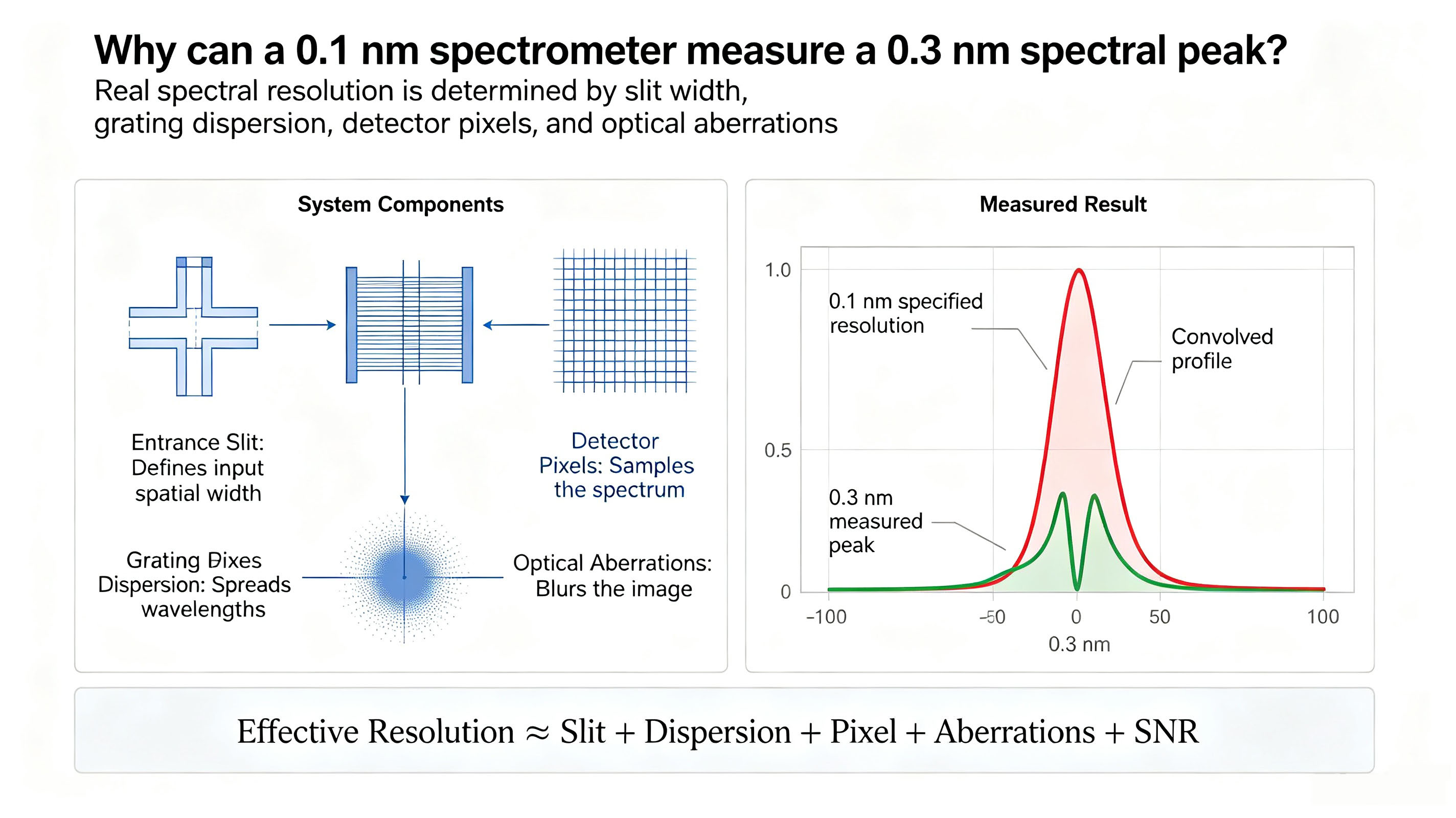
The measured spectral resolution is determined by the entire optical chain, including the entrance slit, diffraction grating, detector, and optical aberrations.
1. Rated Resolution Is Not the Same as Practical Resolution
The resolution specified by a spectrometer manufacturer generally represents a limit or optimum resolution measured under carefully controlled conditions.
Typical conditions may include:
A narrow entrance slit, such as 5–10 μm
A single-line laser source
Long integration time
Minimal optical aberrations
However, laboratory measurements often require very different settings.
For example:
The optical source may be too weak, forcing you to use a 50 μm or 100 μm slit to obtain sufficient optical power.
The sample emission may be weak, limiting the available integration time.
You may install a higher-line-density grating expecting better resolution, but the measured spectrum remains broad.
The underlying problem is that spectral resolution is determined by the complete optical system, not by the grating alone.
2. Why Does the Entrance Slit Matter So Much?
Consider a typical Czerny–Turner spectrometer.
The entrance slit controls the angular range of light entering the diffraction grating.
A wider slit allows a larger range of input angles.
As a result, the same spectral line is spread over a wider range on the detector.
This is known as slit-function broadening.
The combination of slit width and the spectrometer's reciprocal linear dispersion becomes one of the dominant contributors to the measured spectral resolution.
In simple terms:
A high-performance grating cannot fully deliver its theoretical resolution if the entrance slit is too wide.
3. Why Can a 100 μm Slit Turn a 0.05 nm Peak into 0.3 nm?
Let's consider a representative laboratory Czerny–Turner spectrometer.
| Parameter | Typical Value | Description |
|---|---|---|
| Grating groove density | 1200 lines/mm | Common configuration for the visible range |
| Focal length | 250–300 mm | Typical optical path |
| Diffraction order | 1 | Most commonly used |
| Center wavelength | 500 nm | Visible spectral range |
| Reciprocal linear dispersion | ~2.5 nm/mm | Typical value calculated from the grating configuration |
| Entrance slit width | 100 μm | Common setting for weak-light measurements |
| Detector pixel size | 15 μm | Typical linear CCD/CMOS detector |
These representative parameters are taken from the source material.
The calculation is straightforward.
A 100 μm slit is:
100 μm = 0.1 mm
With a reciprocal linear dispersion of approximately:
2.5 nm/mm
the corresponding spectral broadening is:
0.1 mm × 2.5 nm/mm = 0.25 nm
That means the entrance slit alone can contribute approximately 0.25 nm of spectral broadening.
This is already very close to the measured value of 0.3 nm.
Additional broadening can come from detector sampling and optical imperfections.
For example, a 15 μm detector pixel corresponds to approximately:
0.015 mm × 2.5 nm/mm ≈ 0.04 nm
Additional contributions may come from:
Optical aberrations
Collimation errors
Detector sampling
When these effects are combined, a measured linewidth of approximately 0.3 nm becomes entirely reasonable.
The important conclusion is:
The 100 μm entrance slit has already broadened the spectral feature to approximately 0.25 nm before the theoretical resolution of the grating can fully contribute.
This is similar to buying a 4K display but feeding it a 720p signal: the bottleneck is not the display.
4. A Simple Model for Practical Spectral Resolution
The source provides a simplified relationship for estimating the measured resolution:
Δλmeasured ≈ √(Δλslit² + Δλpixel² + Δλaberration²)
where the contributions come from:
Entrance slit broadening
Detector pixel broadening
Optical aberrations
For the representative case:
100 μm slit + 2.5 nm/mm reciprocal linear dispersion
the slit contribution alone is approximately:
0.25 nm
Therefore, even if the diffraction grating has a much higher theoretical resolving capability, the wide entrance slit can prevent the complete optical system from achieving it.
5. Three Different Definitions of Spectral Resolution
A common source of confusion is that engineers may use the word "resolution" to refer to three different things.
5.1 Theoretical Grating Resolution
The theoretical resolving power of a diffraction grating can be expressed as:
R = λ / Δλ = m × N
where:
R is the resolving power
λ is the wavelength
Δλ is the minimum resolvable wavelength difference
m is the diffraction order
N is the total number of illuminated grating grooves
This represents the physical resolving capability of the grating itself.
The source notes that theoretical resolving power can reach approximately 10⁴–10⁶, depending on the grating configuration.
But this is not necessarily the resolution of the complete spectrometer.
5.2 Manufacturer-Rated Resolution
The manufacturer's resolution specification is typically measured using optimized conditions.
For example:
5–10 μm entrance slit + a narrow-linewidth source
may produce a measured FWHM around the specified value, such as:
0.1 nm
This represents the spectrometer's performance under the specified or optimized measurement configuration.
5.3 Actual System Resolution
The resolution that matters in your experiment is the resolution obtained under your actual conditions.
It depends on:
Entrance slit width
Reciprocal linear dispersion
Detector pixel size
Optical aberrations
Alignment
Optical configuration
For the example discussed here, the measured FWHM may be:
0.3 nm
even though the instrument is nominally rated at 0.1 nm.
6. A High-Resolution Grating Does Not Automatically Mean High System Resolution
Suppose a 50 mm-wide diffraction grating has a theoretical resolving power of approximately:
R = 60,000
This means the grating itself may have excellent theoretical resolving capability.
However, in the actual spectrometer:
Only part of the grating may be illuminated.
The entrance slit introduces spectral broadening.
The detector introduces additional sampling limitations.
Optical aberrations further degrade the response.
The source gives an example where the theoretical resolving power of 60,000 can correspond to an actual system resolving power of only approximately 2,000.
This is why simply selecting a higher groove-density grating does not always solve a resolution problem.
The practical resolution can instead be dominated by:
Slit width × reciprocal linear dispersion
and
Pixel size × reciprocal linear dispersion
Whichever contribution is larger can become the dominant bottleneck.
In many practical configurations, a 100 μm entrance slit is the first limitation to investigate.
7. How Can You Make Practical Resolution Approach the Rated Resolution?
If your application requires resolving spectral peaks separated by less than 0.2 nm, the source recommends a practical troubleshooting sequence.
Step 1: Calculate Your Actual Resolution
Do not rely solely on the manufacturer's rated resolution.
Instead, characterize the spectrometer using your actual configuration.
A practical approach is to use a narrow-linewidth laser source, such as a HeNe laser with linewidth below 0.001 nm, and measure the resulting FWHM.
This measured FWHM can be treated as the system response function or practical system resolution.
This is often much more useful than simply reading the resolution number from the datasheet.
8. Step 2: Reduce the Physical Slit Width
There is an unavoidable trade-off between optical throughput and spectral resolution.
The source describes the relationship as:
Higher optical throughput requires a wider slit, while higher resolution requires a narrower slit.
For the representative system, the following settings are suggested:
| Target Resolution | Recommended Slit Width | Approximate Throughput Reduction |
|---|---|---|
| 0.1 nm | ≤20 μm | ~5× |
| 0.05 nm | ≤10 μm | ~10× |
| ~0.3 nm | ~100 μm | Typical weak-light configuration |
The exact performance depends on the spectrometer's optical design and reciprocal linear dispersion, but the general trade-off remains fundamental.
This is one of the most important practical considerations when configuring a spectrometer:
You cannot freely maximize both spectral resolution and optical throughput.
If the signal is weak, narrowing the slit may reduce the detected signal too much.
If the spectral resolution requirement is strict, however, a wide slit may simply be unacceptable.
9. Step 3: Check Whether the Detector Pixel Size Is Adequate
The detector is another potential bottleneck.
A useful engineering rule from the source is:
Pixel size × reciprocal linear dispersion ≤ 1/3 of the target resolution
If detector sampling already consumes a large fraction of the resolution budget, reducing the entrance slit width alone may not be sufficient.
Possible solutions include:
Use a higher groove-density grating
A higher groove density can increase the spectral dispersion and reduce the wavelength range represented by each detector pixel.
Use a longer focal-length spectrometer
A longer focal length can also increase the effective spectral dispersion.
Use a detector with smaller pixels
A detector with smaller pixels can improve spectral sampling and reduce detector-induced broadening.
The correct solution depends on which component is actually limiting the system.
10. Can Grating Angle Improve Spectral Resolution?
The spectral dispersion also depends on the grating geometry.
The source gives the relationship:
dλ/dx = (d × cosβ) / (m × f)
where:
d is the grating period
β is the diffraction angle
m is the diffraction order
f is the focal length
Changing the grating angle and therefore the center wavelength can modify the effective spectral dispersion.
However, in many commercial spectrometers, the grating geometry is determined during manufacturing and is not intended to be adjusted by the end user.
Therefore, if resolution needs to be improved, reducing the entrance slit width is generally the first practical parameter to investigate.
11. The Real Resolution Is a System-Level Parameter
The most important lesson is that spectral resolution should not be treated as a property of the diffraction grating alone.
The practical resolution is determined by the combined effects of:
Entrance slit + diffraction grating + detector + optical aberrations
For the example discussed in this article:
100 μm slit × 2.5 nm/mm reciprocal linear dispersion → approximately 0.25 nm broadening
15 μm detector pixel → approximately 0.04 nm additional broadening
Optical aberrations and alignment errors contribute additional broadening.
Therefore, a spectrometer specified at 0.1 nm can realistically produce a measured FWHM around 0.3 nm under a different slit and measurement configuration.
12. Conclusion
A spectrometer's rated resolution does not automatically represent the resolution you will obtain in every experiment.
If a spectrometer is specified at 0.1 nm, but a 0.05 nm spectral feature appears as approximately 0.3 nm, the first thing to investigate is not necessarily the diffraction grating.
Start with the entrance slit width.
For a representative spectrometer with:
100 μm slit × 2.5 nm/mm reciprocal linear dispersion
the slit alone contributes approximately:
0.25 nm
of spectral broadening.
The detector and optical system then add their own contributions.
The key engineering principle is:
Rated resolution is a specification under defined conditions. Actual resolution is a property of the complete measurement system.
If you need higher practical resolution, check the system in this order:
1. Measure the actual system resolution
2. Reduce the entrance slit width
3. Check detector pixel sampling
4. Evaluate the grating and focal length
5. Check optical aberrations and alignment
In many cases, the most expensive component in the system is not the limiting factor.
You may have a high-performance diffraction grating—but if the entrance slit is too wide, the resolution bottleneck is already at the front door.